New possibilities thanks to our advanced technologies
Home » Technology
Our transparent solar panels are based on perovskite, which increases their efficiency. Transparency allows the surfaces to serve as both an energy source and a window. In addition, our panels allow electric vehicles to go about 20% longer on a single charge. This solution increases the efficiency of existing panels and uses surfaces more efficiently.
The main objective of our research is to develop efficient, semitransparent perovskite solar cells, aiming to enhance both their functionality and flexibility for potential applications in building-integrated photovoltaics (BIPV) and tandem solar cells.
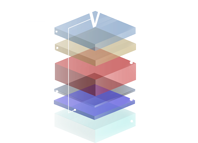
Our fabrication process starts with a transparent glass/FTO (fluorine-doped tin oxide) substrate, providing a conductive foundation. Spin coating is utilized to deposit an electron transport layer (ETL) composed of a compact TiO₂ layer, essential for effective electron extraction and minimizing recombination losses at the interface.
To increase the active interface area between the ETL and the perovskite absorber layer, we apply a mesoporous TiO₂ layer via spin coating, which enhances surface roughness and facilitates more efficient charge transport.
Our fabrication process starts with a transparent glass/FTO (fluorine-doped tin oxide) substrate, providing a conductive foundation. Spin coating is utilized to deposit an electron transport layer (ETL) composed of a compact TiO₂ layer, essential for effective electron extraction and minimizing recombination losses at the interface.
A TiO₂ blocking layer is then deposited using a chemical bath deposition method to improve the interface quality further and inhibit potential backflow of charges, thereby increasing overall efficiency. This blocking layer acts as an additional barrier to reduce electron recombination and supports the stable performance of the cell.
The perovskite layer is then deposited through a spin-coating process. This layer consists of a carefully optimized mixture of methylammonium, formamidinium, cesium, lead, iodine, and bromine ions to balance light absorption, stability, and tunabilityin terms of optical transparency. Achieving the ideal stoichiometry of these components is critical to ensure efficient photon absorption while maintaining a semitransparent structure.
Next, a hole transport layer (HTL) of SPIRO-OMeTAD is deposited atop the perovskite layer to enhance hole mobility and minimize charge recombination, which is crucial for achieving high power conversion efficiency. In the final stage, a layer of gold is deposited as the top contact using the magnetron sputtering technique. This metal contact is precisely calibrated to maintain transparency while providing the necessary conductivity.
To increase the active interface area between the ETL and the perovskite absorber layer, we apply a mesoporous TiO₂ layer via spin coating, which enhances surface roughness and facilitates more efficient charge transport.
A TiO₂ blocking layer is then deposited using a chemical bath deposition method to improve the interface quality further and inhibit potential backflow of charges, thereby increasing overall efficiency. This blocking layer acts as an additional barrier to reduce electron recombination and supports the stable performance of the cell.
The perovskite layer is then deposited through a spin-coating process. This layer consists of a carefully optimized mixture of methylammonium, formamidinium, cesium, lead, iodine, and bromine ions to balance light absorption, stability, and tunabilityin terms of optical transparency. Achieving the ideal stoichiometry of these components is critical to ensure efficient photon absorption while maintaining a semitransparent structure.
Next, a hole transport layer (HTL) of SPIRO-OMeTAD is deposited atop the perovskite layer to enhance hole mobility and minimize charge recombination, which is crucial for achieving high power conversion efficiency. In the final stage, a layer of gold is deposited as the top contact using the magnetron sputtering technique. This metal contact is precisely calibrated to maintain transparency while providing the necessary conductivity.
Following device fabrication, we employ a solar simulator to assess the solar cell’s I-V characteristics and power conversion efficiency (PCE), evaluating the impact of each layer on overall device performance.
Through this structured approach, we aim to establish a reproducible methodology for producing high-efficiency, semitransparent perovskite solar cells, contributingvaluable insights for future development in integrated solar applications.
Following device fabrication, we employ a solar simulator to assess the solar cell’s I-V characteristics and power conversion efficiency (PCE), evaluating the impact of each layer on overall device performance. Through this structured approach, we aim to establish a reproducible methodology for producing high-efficiency, semitransparent perovskite solar cells, contributingvaluable insights for future development in integrated solar applications.
For future work, we aim to enhance the efficiency of our semitransparent perovskite solar cells by optimizing the production environment, focusing on factors such as humidity, temperature control, and precise deposition techniques.
Additionally, we plan to increase the operational lifetime of these cells through advanced encapsulation technologies, which will protect the perovskite layer from environmental factors like moisture and oxygen. This approach is intended not only to improve the durability of the cells but also to ensure their viability for long-term, real-world applications, particularly in building-integrated photovoltaics and other emerging areas of clean energy integration. Additionally, we intend to explore the use of flexible substrates, enabling the deposition of all necessary layers on a bendable foundation. This approach will allow us to develop flexible solar cells, broadening the application scope of our technology for use in wearable electronics, portable energy solutions, and building-integrated photovoltaics
Through these advancements, we aim to push the boundaries of perovskite solar cell durability, versatility, and efficiency. A significant goal moving forward is to scale up the manufacturing process, increasing the cell surface area from sub-square-centimeter dimensions to larger, above-square-centimeter formats. This scale-up will enable broader, commercially viable applications, including integration into larger photovoltaic panels and flexible energy solutions for various real-world applications.
Contact Us